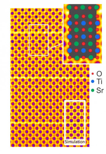
 Colorized sub-Angstrom scanning transmission electron microscope image clearly shows individual atomic columns of strontium (green), titanium (blue), and oxygen (red). A simulated image is overlaid showing close agreement between theory and experiment. The brick and mortar structure is visible.Image Courtesy of: Greg Stone/Penn State(University Park, PA)—Researchers at Penn State and the Molecular Foundry at Lawrence Berkeley National Laboratory are pushing the limits of electron microscopy into the tens of picometer scale, a fraction of the size of a hydrogen atom. The ability to see at this subatomic level is crucial in designing new materials with unprecedented properties, such as materials that transition from metals to semiconductors or that exhibit superconductivity. Their work describing the first atomic scale evidence for strain induced ferroelectricity in a layered oxide appears online today, (August 31), in the journal Nature Communications.
“This paper is important because it highlights our ability to design new classes of materials that can be tuned, one atomic layer at a time, to get interesting new properties such as high frequency tunable dielectrics, which are of interest to the semiconductor industry,” says first author Greg Stone, a former Penn State post-doctoral scholar now at the US Army Research, Development, and Engineering Center.
Designing new materials with potentially useful properties requires the close collaboration of theory, to build mathematical models, synthesis, to create the material in the lab, and characterization, to visualize and measure the material’s properties and provide feedback to tweak theories and improve synthesis.
Related Article: New Electron Microscope Method Detects Atomic-Scale Magnetism
This study builds on previous theoretical work by coauthors Turan Birol and Craig Fennie of Cornell University and experimental work by coauthors Venkatraman Gopalan of Penn State and Darrell Schlom, formerly at Penn State now at Cornell, and their students. Gopalan and Nasim Alem, professors of materials science and engineering at Penn State, led the current study.
Gopalan says, “The material we are looking at is a form of strontium titanate called a layered oxide. This study brings together electron microscopy and density functional theory on a 5-10 picometer length scale to show why these materials are such good tunable dielectrics. The key is phase competition, and for the first time, we show that many polar phases with similar energies compete in this material on the atomic scale, just as theory predicted, which gives it large tunability under a voltage.”
Complex oxides are materials that are formed by the negatively charged oxygen and two other positively charged ions. In this instance, the team examined strontium titanate with a structure called Ruddlesden-Popper (RP), after the two scientists who discovered it. The structure looks like a brick and mortar wall, with the bricks made of the strontium titanate and the thin mortar between the bricks made up of strontium oxide. When the bricks are layered in this fashion, new properties emerge that would not appear in a single brick.
“In the case of RP-strontium titanate, the emergent property is ferroelectricity, which means it has a built-in electrical polarization within its structure. But it could be magnetism or metal-insulator transitions or superconductivity, depending on the atoms involved and the layering order of the materials,” Gopalan says.
Because each layer of brick has a weak connection to other layers, the material can have competing states, with one layer polarized in a direction opposite a neighboring layer. These competing states result in a material with a strong response to a small external stimulus, such as an electric or magnetic field or temperature. In the case of strontium titanate, there is a large dielectric response, which is the ability to store large amounts of energy, as in a capacitor.
Cell phones have many dielectric components that are very small and have to hold a charge. As cell phones transition from 4G networks to 5G, which means they are processing at 5 billion cycles per second, better materials that respond at higher frequencies are crucial. RP-strontium titanate is one such material that is definitely superior to current materials.
Colin Ophus of the National Center for Electron Microscopy facility of the Molecular Foundry says, "This work is an excellent example of the materials advances possible when we close the feedback loop between first principles calculations and atomic resolution electron microscopy."
Related Article: Electron Microscopy Reveals How Vitamin a Enters the Cell
His colleague Jim Ciston at the Molecular Foundry adds, “The precision of the agreement between theory and experiment is critical to unraveling the subtle differences in structure between competing ferroelectric phases. These images of atomic positions are more than pretty pictures of remarkable precision, but contain an enormous amount of quantifiable information about the minute distortions in atomic positions that can lead to surprising properties.”

Lab Management Certificate
The Lab Management certificate is more than training—it’s a professional advantage.
Gain critical skills and IACET-approved CEUs that make a measurable difference.
Additional coauthors on the paper, titled “Atomic Scale Imaging of Competing Polar States in a Ruddleston-Popper Layered Oxide,” were Nasim Alem, assistant professor of materials science and engineering, Penn State, Turan Birol, Fennie’s Ph.D. student now assistant professor at University of Minnesota, Che-Hui Lee, Schlom’s Ph.D. student at Penn State and Cornell, and Penn State staff scientist Ke Wang.
Support was provided through the Penn State Center for Nanoscale Science, a National Science Foundation Materials Research Science and Engineering Center (MRSEC), the Department of Energy and the Rutgers Center for Materials Theory. Work at the Molecular Factory was supported by the Office of Science, Office of Basic Energy Sciences, of the U. S. Department of Energy. Portions of the work were performed in the Penn State electron microscopy facilities in Penn State’s Materials Research Institute.
Contact: Prof. Venkatraman Gopalan vxg8@psu.edu