
An international team of researchers, affiliated with Ulsan National Institute of Science and Technology (UNIST) has unveiled a novel material that could enable major leaps in the miniaturization of electronic devices. Published in the journal Nature, this study represents a significant achievement for future electronics.
This breakthrough comes from a research, conducted by professor Hyeon Suk Shin (School of Natual Sciences, UNIST) and principal researcher Dr. Hyeon-Jin Shin from Samsung Advanced Institute of Technology (SAIT), in collaboration with Graphene Flagship researchers from University of Cambridge (UK) and Catalan Institute of Nanoscience and Nanotechnology (ICN2, Spain).
In this study, the team successfully demonstrated the synthesis of thin film of amorphous boron nitride (a-BN) with extremely low dielectric constant as well as high breakdown voltage and superior metal barrier properties. The research team noted that this newly fabricated material has great potential as interconnect insulators in the next-generation of electronic circuits.

In the ongoing process of miniaturization of logic and memory devices in electronic circuits, minimizing the dimensions of interconencts—metal wires that link the different device components on the chip—is crucial to guarantee improved performance and faster response of the device. Extensive research efforts have been devoted to decreasing the resistance of scaled interconnects because integration of dielectrics using complementary metal oxide semiconductor (CMOS) compatible processes has proven to be exceptionally challenging. According to the research team, the required interconnect isolation materials should not only possess low relative dielectric constants (referred to as k-values), but should also be thermally, chemically, and mechanically stable.


There has been an ongoing quest to obtain materials with ultra-low-k (relative permittivity around or below 2) avoiding the artificial addition of pores in the thin film in the semiconductor industry for at least the past 20 years. Several attempts had been made to develop materials with desired characteristics, yet those materials have failed to be successfully integrated in interconnects due to poor mechanical properties or poor chemical stability upon integration, causing reliability failures.
Related Article: New Material, Picked by Computers, Could Boost Power of Vacuum Electronics
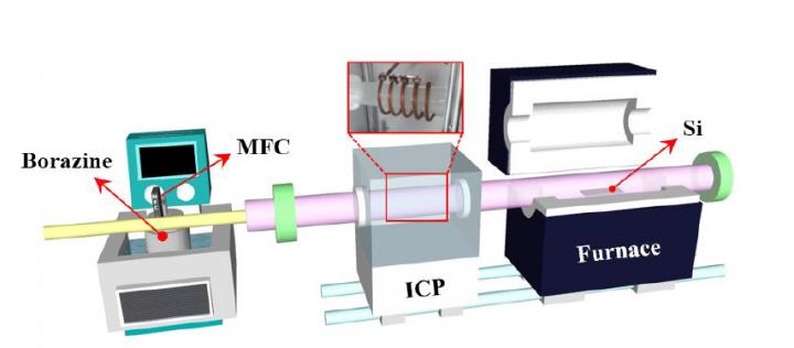
In this study, the joint research has succeeded in demonstrating a back-end-of-the-line (BEOL) compatible approach to grow amorphous boron nitride (a-BN) with extremely low-k dielectrics. In particular, they synthesized approximately 3 nm thin a-BN on a Si substrate, using low temperature remote inductively coupled plasma-chemical vapor deposition (ICP-CVD). The resulting material showed an extremely low dielectric constant in the range of 1.78, which is 30 percent lower than the dielectric constant of currently available insulators.
"We found that temperature was the most important parameter with ideal a-BN film deposition occurring at 400° C," says Seokmo Hong, who is in the doctoral program of natural sciences and the first author of the study. "This material with ultra-low-k also manifests a high breakdown voltage and likely superior metal barrier properties, making the film very attractive for practical electronic applications."
Angle-dependent near-edge X-ray absorption fine structure (NEXAFS) measured in partial electron-yield (PEY) mode at Pohang Light Source-II 4D beam line was also used to investigate the chemical and electronic structures of a-BN. Their findings indicated that the irregular, random atomic arrangement causes the dielectric constant value to drop.
The new material also manifests excellent mechanical properties of high strength. Moreover, when researchers tested the diffusion barrier properties of a-BN in very harsh conditions, they found it can prevent metal atom migration from the interconnects into the insulator. This result will help resolves a long-standing issue of interconnects in CMOS integrated circuit fabrication, enabling further miniaturization of electronic devices.
"Development of electrically, mechanically and thermally robust low-k materials (k < 2) has long been technically challenging," says Shin. "Our research is also a great example that shows companies and academic institutions working together to create greater synergy.
Our results demonstrate that the amorphous counterpart of two-dimensional hexagonal BN possesses the ideal low-k dielectric characteristics for high-performance electronics. If they are commercialized, it will be a great help in overcoming the crisis looming over the semiconductor industry."


