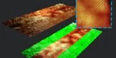
 Researchers at Argonne’s Center for Nanoscale Materials have confirmed the growth of self-directed graphene nanoribbons on the surface of the semiconducting material germanium by researchers at the University of Wisconsin at Madison.Image courtesy of Argonne National LaboratoryIn a development that could revolutionize electronic circuitry, a research team from the University of Wisconsin at Madison (UW) and the U.S. Department of Energy's Argonne National Laboratory has confirmed a new way to control the growth paths of graphene nanoribbons on the surface of a germainum crystal.
Germanium is a semiconductor, and this method provides a straightforward way to make semiconducting nanoscale circuits from graphene, a form of carbon only one atom thick.
The method was discovered by UW scientists and confirmed in tests at Argonne.
"Some researchers have wanted to make transistors out of carbon nanotubes, but the problem is that they grow in all sorts of directions," said Brian Kiraly of Argonne. "The innovation here is that you can grow these along circuit paths that works for your tech."
UW researchers used chemical vapor deposition to grow graphene nanoribbons on germanium crystals. This technique flows a mixture of methane, hydrogen, and argon gases into a tube furnace. At high temperatures, methane decomposes into carbon atoms that settle onto the germanium's surface to form a uniform graphene sheet. By adjusting the chamber's settings, the UW team was able to exert very precise control over the material.
"What we've discovered is that when graphene grows on germanium, it naturally forms nanoribbons with these very smooth, armchair edges," said Michael Arnold, an associate professor of materials science and engineering at UW-Madison. "The widths can be very, very narrow, and the lengths of the ribbons can be very long, so all the desirable features we want in graphene nanoribbons are happening automatically with this technique."
Graphene, a one-atom-thick, two-dimensional sheet of carbon atoms, is known for moving electrons at lightning speed across its surface without interference. This high mobility makes the material an ideal candidate for faster, more energy-efficient electronics.
However, the semiconductor industry wants to make circuits start and stop electrons at will via band-gaps, as they do in computer chips. As a semimetal, graphene naturally has no band-gaps, making it a challenge for widespread industry adoption. Until now.
To confirm these findings, UW researchers went to Argonne staff scientists Brian Kiraly and Nathan Guisinger at the Center for Nanoscale Materials, a DOE Office of Science User Facility located at Argonne.
"We have some very unique capabilities here at the Center for Nanoscale Materials," said Guisinger. "Not only are our facilities designed to work with all different sorts of materials from metals to oxides, we can also characterize, grow and synthesize materials."
Using scanning tunneling microscopy, a technique using electrons (instead of light or the eyes) to see the characteristics of a sample, researchers confirmed the presence of graphene nanoribbons growing on the germanium. Data gathered from the electron signatures allowed the researchers to create images of the material's dimensions and orientation. In addition, they were able to determine its band structure and extent to which electrons scattered throughout the material.
"We're looking at fundamental physical properties to verify that it is, in fact, graphene and it shows some characteristic electronic properties," said Kiraly. "What's even more interesting is that these nanoribbons can be made to grow in certain directions on one side of the germanium crystal, but not the other two sides."
For use in electronic devices, the semiconductor industry is primarily interested in three faces of a germanium crystal. Depicting these faces in terms of coordinates (X,Y,Z), where single atoms connect to each other in a diamond-like grid structure, each face of a crystal (1,1,1) will have axes that differ from one (1,1,0) to the other (1,0,0).
Previous research shows that graphene sheets can grow on germanium crystal faces (1,1,1) and (1,1,0). However, this is the first time any study has recorded the growth of graphene nanoribbons on the (1,0,0) face.
As their investigations continue, researchers can now focus their efforts on exactly why self-directed graphene nanoribbons grow on the (1,0,0) face and determine if there is any unique interaction between the germanium and graphene that may play a role.
This research is detailed in the paper "Direct oriented growth of armchair graphene nanoribbons on germanium," published in Nature Communications. The method for this work was led by Michael Arnold's Advanced Materials for Energy and Electronics Group at UW-Madison. Confirmation of findings was led by Nathan Guisinger and Brian Kiraly at the Center for Nanoscale Materials at Argonne National Laboratory. Additional co-authors include Robert M. Jacobberger, Matthieu Fortin-Deschenes, Pierre L. Levesque, Kyle M. McElhinny, Gerald J. Brady, Richard Rojas Delgado, Susmit Singha Roy, Andrew Mannix, Max G. Lagally, Paul G. Evans, Patrick Desjardins, Richard Martel and Mark C. Hersam.
This work was supported in part by the U.S. Department of Energy’s Office of Science, the Natural Science and Engineering Research Council, the University of Wisconsin Materials Research Science and Engineering Center, the Department of Defense Air Force Office of Scientific Research, and the National Science Foundation’s Graduate Research Fellowships.


