 Using the supercomputing resources at the Argonne Leadership Computing Facility, University of Chicago and Argonne researchers have found a way miniaturize microchip components using a technique producing zero defects. This advance will allow semiconductor manufacturers to meet miniaturization target dates to produce smaller components with added functionality for our favorite devices.Image courtesy of Argonne National LaboratoryTarget dates are critical when the semiconductor industry adds small, enhanced features to our favorite devices by integrating advanced materials onto the surfaces of computer chips. Missing a target means postponing a device's release, which could cost a company millions of dollars or, worse, the loss of competitiveness and an entire industry. But meeting target dates can be challenging because the final integrated devices, which include billions of transistors, must be flawless—less than one defect per 100 square centimeters.
Researchers at the University of Chicago and the U.S. Department of Energy's (DOE's) Argonne National Laboratory, led by Juan de Pablo and Paul Nealey, may have found a way for the semiconductor industry to hit miniaturization targets on time and without defects.
Related article: A Different Type of 2D Semiconductor
To make microchips, de Pablo and Nealey's technique includes creating patterns on semiconductor surfaces that allow block copolymer molecules to self-assemble into specific shapes, but thinner and at much higher densities than those of the original pattern. The researchers can then use a lithography technique to create nano-trenches where conducting wire materials can be deposited.
This is a stark contrast to the industry practice of using homo-polymers in complex "photoresist" formulations, where researchers have "hit a wall," unable to make the material smaller.
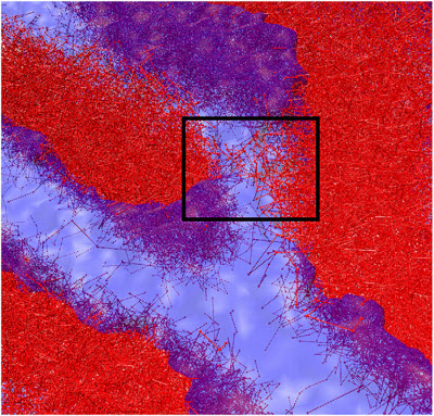
Before they could develop their new fabrication method, however, de Pablo and Nealey needed to understand exactly how block copolymers self-assemble when coated onto a patterned surface—their concern being that certain constraints cause copolymer nanostructures to assemble into undesired metastable states. To reach the level of perfection demanded to fabricate high-precision nanocircuitry, the team had to eliminate some of these metastable states.
Related article: Scientists Craft a Semiconductor Junction Only Three Atoms Thick
To imagine how block copolymers assemble, it may be helpful to picture an energy landscape consisting of mountains and valleys where some valleys are deeper than others. The system prefers defect-free stability, which can be characterized by the deepest (low-energy) valleys, if they can be found. However, systems can get trapped inside higher (medium energy) valleys, called metastable states, which have more defects.
To move from a metastable to stable state, block copolymer molecules must find ways to climb over the mountains and find lower energy valleys.
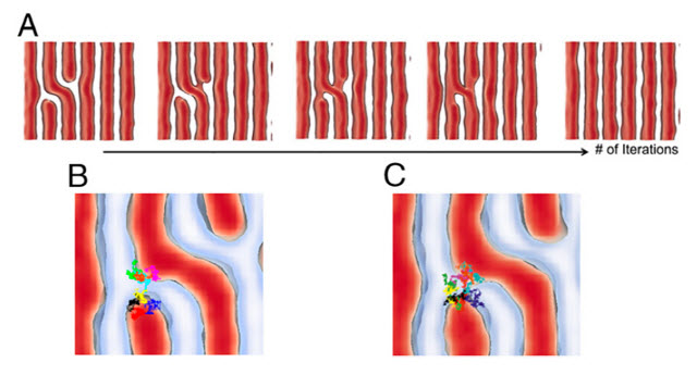
 Researchers from the University of Chicago and Argonne use the supercomputing resources at the Argonne Leadership Computing Facility to predict the path molecules must follow to find defect-free states and designed a process that delivers industry-standard nanocircuitry that can be scaled down to smaller densities without defects.Image courtesy of Argonne National Laboratory"Molecules in these metastable states are comfortable, and they can remain in that state for extraordinarily long periods of time," said de Pablo of the University of Chicago's and Argonne's Institute for Molecular Engineering. "In order to escape such states and attain a perfect arrangement, they need to start rearranging themselves in a manner that allows the system to climb over local energy barriers, before reaching a lower energy minimum. What we have done in this work is predict the path these molecules must follow to find defect-free states and designed a process that delivers industry-standard nanocircuitry that can be scaled down to smaller densities without defects."
Using an INCITE grant, de Pablo and his team used the Mira and Fusion supercomputers at the Argonne Leadership Computing Facility, a DOE Office of Science User Facility. There, the team generated molecular simulations of self-assembling block polymers along with sophisticated sampling algorithms to calculate where barriers to structural rearrangement would arise in the material.
After all the calculations were done, the researchers could precisely predict the pathways of molecular rearrangement that block copolymers must take to move from a metastable to stable state. They could also experiment with temperatures, solvents and applied fields to further manipulate and decrease the barriers between these states.
Related article: Beyond Silicon: Transistors without Semiconductors
To test these calculations, de Pablo and Nealey partnered with IMEC, an international consortium located in Belgium. Their commercial-grade fabrication and characterization instruments helped the researchers perform experiments under conditions that are not available in academic laboratories. An individual defect measures only a handful of nanometers; "finding a defect in a 100 square centimeter area is like finding a needle in hay stack, and there are only a few places in the world where one has access to the necessary equipment to do so," says de Pablo.
"Manufacturers have long been exploring the feasibility of using block copolymer assembly to reach the small critical dimensions that are demanded by modern computing and higher data storage densities," de Pablo said. "Their biggest challenge involved evaluating defects; by following the strategies we have outlined, that challenge is greatly diminished."
John Neuffer, president and CEO of the Semiconductor Industry Association (SIA), says industry is relentlessly focused on designing and building chips that are smaller, more powerful and more energy-efficient. "The key to unlocking the next generation of semiconductor innovation is research," he said. "SIA commends the work done by Argonne National Laboratory and the University of Chicago, as well as other critical scientific research being done across the United States."
De Pablo, Nealey and their team will continue their investigations with a wider class of materials, increasing the complexity of patterns and characterizing materials in greater detail while also developing methods based on self-assembly for fabrication of three-dimensional structures.
Their long-term goal, with support from the DOE's Office of Science, is to arrive at an understanding of directed self-assembly of polymeric molecules that will enable creation of wide classes of materials with exquisite control over their nanostructure and functionality for applications in energy harvesting, storage and transport.