Electrons can extend our view of microscopic objects well beyond what’s possible with visible light—all the way to the atomic scale. A popular method in electron microscopy for looking at tough, resilient materials in atomic detail is called STEM, or scanning transmission electron microscopy, but the highly focused beam of electrons used in STEM can also easily destroy delicate samples.
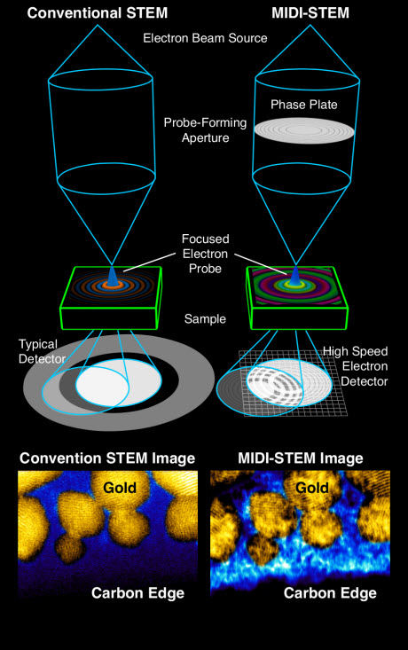 In MIDI-STEM (right), developed at Berkeley Lab, an electron beam travels through a ringed “phase plate,” producing a high-resolution image (bottom right) that provides details about a sample containing a heavy element (gold) and light element (carbon). Details about the carbon are missing in an image (bottom left) of the sample using a conventional electron imaging technique (ADF-STEM).Image credit: Colin Ophus/Berkeley Lab, Nature Communications: 10.1038/ncomms10719This is why using electrons to image biological or other organic compounds, such as chemical mixes that include lithium—a light metal that is a popular element in next-generation battery research—requires a very low electron dose.
Scientists at the Department of Energy’s Lawrence Berkeley National Laboratory (Berkeley Lab) have developed a new imaging technique, tested on samples of nanoscale gold and carbon, that greatly improves images of light elements using fewer electrons.
The newly demonstrated technique, dubbed MIDI-STEM, for matched illumination and detector interferometry STEM, combines STEM with an optical device called a phase plate that modifies the alternating peak-to-trough, wave-like properties (called the phase) of the electron beam.
This phase plate modifies the electron beam in a way that allows subtle changes in a material to be measured, even revealing materials that would be invisible in traditional STEM imaging.
Related Article: Imaging Systems for Biology: Responding to Multidisciplinary Needs
Another electron-based method, which researchers use to determine the detailed structure of delicate, frozen biological samples, is called cryo-electron microscopy, or cryo-EM. While single-particle cryo-EM is a powerful tool—it was named as science journal Nature’s 2015 Method of the Year—it typically requires taking an average over many identical samples to be effective. Cryo-EM is generally not useful for studying samples with a mixture of heavy elements (for example, most types of metals) and light elements like oxygen and carbon.
“The MIDI-STEM method provides hope for seeing structures with a mixture of heavy and light elements, even when they are bunched closely together,” said Colin Ophus, a project scientist at Berkeley Lab’s Molecular Foundry and lead author of a study, published Feb. 29 in Nature Communications, that details this method.
If you take a heavy-element nanoparticle and add molecules to give it a specific function, conventional techniques don’t provide an easy, clear way to see the areas where the nanoparticle and added molecules meet.
“How are they aligned? How are they oriented?” Ophus asked. “There are so many questions about these systems, and because there wasn’t a way to see them, we couldn’t directly answer them.”
While traditional STEM is effective for “hard” samples that can stand up to intense electron beams, and cryo-EM can image biological samples, “We can do both at once” with the MIDI-STEM technique, said Peter Ercius, a Berkeley Lab staff scientist at the Molecular Foundry and co-author of the study.
The phase plate in the MIDI-STEM technique allows a direct measure of the phase of electrons that are weakly scattered as they interact with light elements in the sample. These measurements are then used to construct so-called phase-contrast images of the elements. Without this phase information, the high-resolution images of these elements would not be possible.
In this study, the researchers combined phase plate technology with one of the world’s highest resolution STEMs, at Berkeley Lab’s Molecular Foundry, and a high-speed electron detector.
They produced images of samples of crystalline gold nanoparticles, which measured several nanometers across, and the superthin film of amorphous carbon that the particles sat on. They also performed computer simulations that validated what they saw in the experiment.
The phase plate technology was developed as part of a Berkeley Lab Laboratory Directed Research and Development grant in collaboration with Ben McMorran at University of Oregon.
The MIDI-STEM technique could prove particularly useful for directly viewing nanoscale objects with a mixture of heavy and light materials, such as some battery and energy-harvesting materials, that are otherwise difficult to view together at atomic resolution.
It also might be useful in revealing new details about important two-dimensional proteins, called S-layer proteins, that could serve as foundations for engineered nanostructures but are challenging to study in atomic detail using other techniques.
In the future, a faster, more sensitive electron detector could allow researchers to study even more delicate samples at improved resolution by exposing them to fewer electrons per image.
“If you can lower the electron dose you can tilt beam-sensitive samples into many orientations and reconstruct the sample in 3-D, like a medical CT scan. There are also data issues that need to be addressed,” Ercius said, as faster detectors will generate huge amounts of data. Another goal is to make the technique more “plug-and-play,” so it is broadly accessible to other scientists.
Berkeley Lab’s Molecular Foundry is a DOE Office of Science User Facility. Researchers from the University of Oregon, Gatan Inc., and Ulm University in Germany also participated in the study.