semiconductors

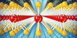
In 2013 James Hone, Wang Fong-Jen Professor of Mechanical Engineering at Columbia Engineering, and colleagues at Columbia demonstrated that they could dramatically improve the performance of graphene—highly conducting two-dimensional (2D) carbon—by encapsulating it in boron nitride (BN), an insulating material with a similar layered structure. In work published this week in the Advance Online Publication on Nature Nanotechnology’s website, researchers at Columbia Engineering, Harvard, Cornell, University of Minnesota, Yonsei University in Korea, Danish Technical University, and the Japanese National Institute of Materials Science have shown that the performance of another 2D material—molybdenum disulfide (MoS2)—can be similarly improved by BN-encapsulation.

University of Washington scientists have built a new nanometer-sized laser — using the thinnest semiconductor available today — that is energy efficient, easy to build and compatible with existing electronics.

Engineers at the University of Texas at Dallas have created semiconductor technology that could make night vision and thermal imaging affordable for everyday use.

The University of Alabama in Huntsville (UAH) has partnered with four other research universities and a consortium of photonics industry leaders in an effort to win a $110 million federal contract for an integrated photonics institute that would be housed in the $70 million Florida Advanced Manufacturing Research Center (FAMRC) being built near Kissimmee, Fla.

Collaboration with Lund University uses modified University of Oregon spectroscopy equipment to study 'maze' of connections in photoactive quantum dots.


