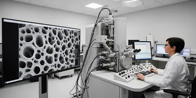
Electron microscopy represents a cornerstone of modern scientific inquiry, providing unparalleled insights into the structure and properties of matter at the nanoscale. Its foundational principle—the use of a focused electron beam instead of light—enables a resolution far surpassing that of conventional light microscopes, making it an indispensable tool for material science, biology, chemistry, and engineering. The interaction of high-energy electrons with a specimen produces various signals, including scattered electrons, characteristic X-rays, and cathodoluminescence, each providing unique information about the sample's morphology, composition, and crystal structure.
The selection of an appropriate electron microscopy technique is not a one-size-fits-all solution but a strategic decision based on the specific research question. A thorough understanding of the principles, capabilities, and limitations of each method is crucial for obtaining meaningful and accurate results. This comprehensive overview of electron microscopy techniques offers a guide for laboratory professionals to navigate these complex choices, ensuring the optimal approach is employed for any given analysis.
Scanning Electron Microscopy (SEM) for Detailed Surface Analysis
Scanning electron microscopy (SEM) is a powerful and widely utilized electron microscopy technique for the examination of a specimen's surface topography and morphology. The instrument operates by scanning a finely focused beam of electrons across the sample. As the primary electrons interact with the atoms in the specimen, they generate various signals that are collected by detectors to form an image. The most common signals used for imaging are secondary electrons (SE) and backscattered electrons (BSE).
Secondary electrons are low-energy electrons emitted from the very surface of the sample. The yield of these electrons is highly sensitive to the sample's surface geometry, providing high-resolution, three-dimensional-like images of the specimen's topography. This capability makes SEM invaluable for studying surfaces, fractures, powders, and a vast range of material structures.
Backscattered electrons, in contrast, are high-energy primary electrons that have been elastically scattered back from the sample. The yield of BSE is strongly dependent on the atomic number of the atoms in the specimen. Consequently, BSE imaging provides a strong compositional contrast, allowing for the differentiation of phases and the identification of material interfaces based on elemental composition.
- Principle of Operation: A focused electron beam scans the sample surface in a rectangular pattern. Detectors collect signals (SE, BSE) generated by electron-sample interactions. The signal intensity at each point is then mapped to a corresponding pixel on a display screen, building a detailed image.

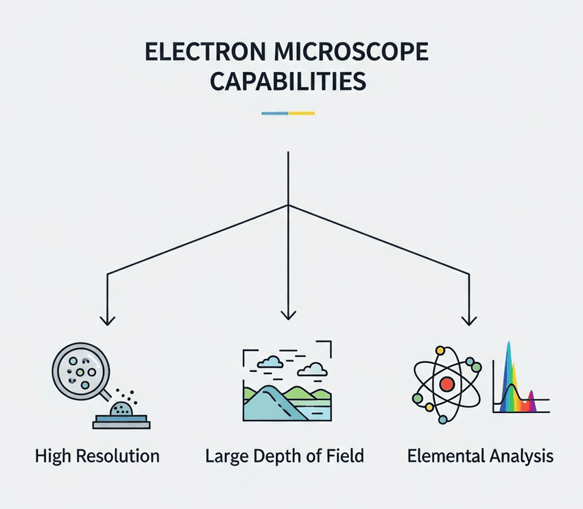
Used correctly, the electron microscope can have a variety of uses.
GEMINI (2025)
- Key Capabilities:
- High-resolution imaging of surface morphology and topography.
- Large depth of field, resulting in images with a distinct three-dimensional appearance.
- Elemental analysis, particularly when coupled with an Energy-Dispersive X-ray Spectroscopy (EDS or EDX) detector, which identifies elements based on characteristic X-rays emitted from the sample.
- Ideal Applications for SEM:
- Examining fracture surfaces in metallurgy and materials science.
- Analyzing the surface texture of biological specimens.
- Quality control for microfabricated devices and integrated circuits.
- Assessing the porosity and structure of geological and ceramic materials.
SEM's versatility and relatively straightforward sample preparation make it a primary tool for a wide range of analytical needs. Its ability to provide both morphological and compositional information in a single platform makes it a workhorse for material imaging.
Transmission Electron Microscopy (TEM) for Internal Structure and Crystallography
Transmission electron microscopy (TEM) provides a complementary perspective to SEM by enabling the examination of a specimen's internal structure with exceptional resolution. Unlike SEM, TEM requires the electron beam to pass through the specimen. To achieve this, samples must be prepared to be ultrathin—typically less than 100 nanometers—to be electron-transparent.
As the electrons traverse the specimen, some are scattered by the atoms. The transmitted and scattered electrons are then collected by an objective lens and projected onto a fluorescent screen or a digital detector to form a magnified image. The information gained from TEM can be broadly categorized into two types of imaging: Bright-Field (BF) and Dark-Field (DF) imaging, which reveal structural and defect information, and electron diffraction, which provides crystallographic data.
A key advantage of TEM is its ability to achieve atomic-scale resolution, allowing for the visualization of individual atomic columns in crystalline materials. This capability is vital for studying crystal lattice defects, grain boundaries, and the structure of nanoparticles. The information derived from TEM is crucial for understanding the fundamental relationship between a material's atomic structure and its properties.
Feature | Scanning Electron Microscopy (SEM) | Transmission Electron Microscopy (TEM) |
|---|---|---|
Information Gained | Surface morphology, topography, composition | Internal structure, crystallography, lattice defects |
Resolution | Typically 0.5–20 nanometers | Typically 0.05–0.2 nanometers |
Sample Preparation | Less demanding (e.g., coating, mounting) | Highly demanding (ultrathinning, polishing) |
Magnification Range | 10x to 1,000,000x | 50x to 10,000,000x |
Working Environment | High vacuum | Ultra-high vacuum |
Advanced Electron Microscopy Techniques for Specialized Analysis
While SEM and TEM are the primary pillars of electron microscopy, several advanced techniques have been developed to address highly specific analytical challenges. These methods often build upon the core principles of SEM and TEM to provide deeper insights into a material's chemical, electronic, or magnetic properties.
Scanning Transmission Electron Microscopy (STEM) is a prime example, combining aspects of both SEM and TEM. In STEM, a finely focused electron probe is scanned across an ultrathin sample, similar to SEM. However, instead of detecting scattered electrons from the surface, detectors placed beneath the sample collect the transmitted electrons. This mode of operation allows for high-resolution imaging and elemental mapping, as it can be combined with spectroscopic techniques like Electron Energy Loss Spectroscopy (EELS) and Energy-Dispersive X-ray Spectroscopy (EDS).
Electron Energy Loss Spectroscopy (EELS) is a powerful analytical technique that measures the energy lost by electrons as they pass through a sample. This energy loss is characteristic of the elements present and their chemical bonding states. EELS offers superior spatial resolution and sensitivity to light elements (like lithium, carbon, and nitrogen) compared to EDS, making it an invaluable tool for battery research, catalysis, and carbon-based materials.
Cryo-Electron Microscopy (Cryo-EM) has revolutionized structural biology. It involves flash-freezing biological samples in a thin layer of amorphous ice to preserve their native, hydrated state. The frozen sample is then imaged with a TEM, and thousands of two-dimensional images are computationally reconstructed to generate a high-resolution, three-dimensional model of the macromolecule or cellular component. This method has enabled the visualization of complex protein structures that are challenging to crystallize for X-ray crystallography, leading to significant advancements in drug discovery and molecular biology. These advanced microscopy techniques demonstrate the continuous evolution of electron microscopy as a tool for comprehensive material imaging.
Optimizing Sample Preparation for High-Quality Microscopy
The quality of an electron microscopy analysis is profoundly dependent on the preparation of the specimen. Proper sample preparation is not merely a procedural step but a critical component of the overall experimental design. An inadequately prepared sample can introduce artifacts that obscure the true structure, leading to erroneous interpretations.
For SEM, sample preparation often involves mounting the specimen and, for non-conductive materials, applying a thin coating of a conductive material like gold or carbon. This coating prevents charging effects that can distort images and degrade resolution. Techniques such as sputter coating are standard for this purpose. For biological samples, chemical fixation and dehydration are necessary to preserve cellular structures and withstand the high vacuum of the microscope.
TEM sample preparation is significantly more intricate due to the requirement for electron transparency. Materials scientists often employ techniques like mechanical polishing, focused ion beam (FIB) milling, or ultramicrotomy to create ultrathin sections. FIB milling is particularly powerful as it allows for the precise extraction of a thin lamella from a specific region of interest, preserving the integrity of the surrounding structure. Biological specimens are typically embedded in a resin and then sliced with an ultramicrotome, followed by heavy metal staining to enhance contrast. The skill and precision applied during sample preparation are instrumental in achieving high-resolution, artifact-free images, directly impacting the validity of the final research findings.
Selecting the Optimal Electron Microscopy Method
The final choice among various electron microscopy techniques hinges on a clear understanding of the analytical goals. For studies focused on surface morphology and topography, scanning electron microscopy is the ideal choice. Its ability to provide three-dimensional-like images and handle bulk samples makes it the go-to technique for a vast array of applications, including failure analysis and surface characterization. When the research question pertains to the internal atomic structure, crystal defects, or the composition of nanoscale features, transmission electron microscopy is the more appropriate method. Its superior resolution and ability to perform diffraction analysis provide the atomic-level detail necessary for advanced material science and nanotechnology.
For highly specialized inquiries, techniques like STEM and EELS offer a powerful combination of spatial resolution and chemical analysis, while Cryo-EM provides a unique solution for visualizing delicate biological structures in their native state. The continuous advancement of electron microscopy ensures that researchers have a diverse toolkit for probing the fundamental properties of matter, driving innovation across scientific disciplines.
Frequently Asked Questions about Electron Microscopy
What is the primary difference between SEM and TEM?
The core distinction lies in how the electron beam interacts with the sample. SEM analyzes scattered electrons from the surface, providing information on topography and composition, while TEM uses electrons that pass through an ultrathin sample to reveal internal structure and crystallography.
Why is sample preparation so critical in material imaging?
Proper sample preparation is essential to prevent artifacts that can distort images and lead to incorrect data interpretation. For electron microscopy, specimens must be stable and, for TEM, electron-transparent to ensure accurate and high-resolution imaging of the material.
Can electron microscopy be used for chemical analysis?
Yes. Both SEM and TEM can be equipped with detectors for techniques like Energy-Dispersive X-ray Spectroscopy (EDS/EDX) and Electron Energy Loss Spectroscopy (EELS). These methods identify the elemental composition and chemical bonding of materials, providing comprehensive insights into their properties.
What are the main advantages of electron microscopy over light microscopy?
The primary advantage is vastly superior resolution and magnification. Electron microscopes can resolve details down to the atomic scale, whereas light microscopy is limited by the wavelength of light. This makes electron microscopy indispensable for high-resolution material imaging and nanoscale research.


