Materials Science

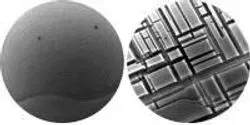
Rust never sleeps. Whether a reference to the 1979 Neil Young album or a product designed to protect metal surfaces, the phrase invokes the idea that corrosion from oxidation—the more general chemical name for rust and other reactions of metal with oxygen—is an inevitable, persistent process. But a new study performed at the Center for Functional Nanomaterials (CFN) at the U.S. Department of Energy's (DOE) Brookhaven National Laboratory reveals that certain features of metal surfaces can stop the process of oxidation in its tracks.

Innovative optical fiber developed by researchers from Clemson University, the University of Wisconsin-Milwaukee, the University of New Mexico and Corning Incorporated was chosen as one of Physics World’s Top Ten Breakthroughs of 2014.

X-ray photoelectron spectroscopy (XPS) is one of the most sensitive and informative surface analysis techniques available. However, XPS requires a high vacuum to operate, which makes analyzing materials in liquid and gaseous environments difficult.

In 2014, Lawrence Livermore National Laboratory (LLNL) built on a 62-year tradition of translating basic science into technologies that ensure national security, address pressing real world problems and expand the boundaries of fundamental science.

Collaboration with Lund University uses modified University of Oregon spectroscopy equipment to study 'maze' of connections in photoactive quantum dots.


